Electronic Devices Research and Development Laboratory
“Make real what few years earlier was only imaginable or barely possible”
Modern connected word, availability of techniques, tools, gain in open and free software open for us new design approaches which we love to explore and utilize in our work.
About us
Dependable partner in electronic device design
LABiRUE in Polish “Laboratorium Badań i Rozwoju Urządzeń Elektronicznych” is electronic device {research, design, prototyping, test and improvement } bureau operated by professional passionates engineers. Mixture of well interdyscyplinarny oriented people with broad range of interests.
We are located in southern part of Poland in the center of Silesian Metropolitan Area.
We believe that in modern word innovation happen mostly on the domain borders so we are open to work with you.
More than 10+ years of professional experience
Professional design, experience obtained in automotive and industrial automation secotrs.
An individual approach
We understand different organizations structures and their demands from big corporation down to small businesses.
Flat, vital organization structure
Our organization let us elastically select methods and tools according to current demands improving overall workflow!
Faster to the goals
In house design, build, test and improvement processes with minimization of external dependencies eliminates time delays.
Know OUR CAPABILITIES
Where Full‑Stack Engineering, Comes Together
In the following blocks you can know more about our particular working and design practices.
System architecture design
We prefer having horizontal view on product we design. The better we understand application better we can imagine future problems and we may offer better solution. We have experience in hardware embedded systems and also software architecture for automotive and industrial.
Design Calculations
Design calculations have to document and prove chosen circuit topologies and component values. Tools like Excel, Mathcad and their alternatives are heavily used.
Hardware cost optimization
Rational components and technologies selection for long availability, swapability also with 6Sigma quality help to not overdesign and improve overall manufacturability, yield and product longevity during device lifecycle.
Analog/Power Circuit design
Basis of each stable system is power network. We design flyback, DCDC, low noise power supplies with sequencing required by various SoC and FPGA, BMSes, chargers.
Key interface to physical analog word are different kind of filters, amplifiers, sensors and signal shaping stages which we also design.
Digital/Programmable Circuit design
We know high speed interfaces: I2C, SMBus, SPI, CAN, LIN, QSPI, MIPI CSI/DSI, SGMII, RGMII, GMSL SDCard, DDR, PCIExpress. We work with SoC like TI Sitara, NXP IMX, Layerscape, MEDIATEK Genio + FPGAs. Microcontrollers AVR, STM8, STM32, TI Picollo.
Some high relability related system still need realize part of safety monitoring or armoring circuit in digital logic. Sometimes there is need for special sequencing of multiple power supplies different for power up and down. We realize it “bare in metal” or as small programeable logic devices from Cypress.
Schematic capture & Printed circuit board layout
Clean schematic and its partitioning, modularity is key for understable, good design practice which we follow. Proper material selection like component packages imposes requirements onto printed circuit board technology and assembly accuracy. Proper and wise components/block placement, signals routing with board layout simulations help to eliminate signal integrity or EMC problems. Our own designs we perfer handling with KiCad but we also know Siemens Expedition design tools.
Embedded firmware
We develop complete embedded‑firmware stacks — from bare‑metal micro controller code, real‑time control logic up to embedded Linux drivers, BSP bring‑up, secure bootloaders, connectivity stacks. Vertical alignment with hardware allow us optimize our firmware for ultra‑low‑power architectures.
Our team delivers deterministic, safe, maintainable and production‑ready firmware for embedded systems which can satisfy rigorous automotive industry standards.
Prototyping, low volume production
Our prototyping shop allows us to locally create untypical tooling and masks.
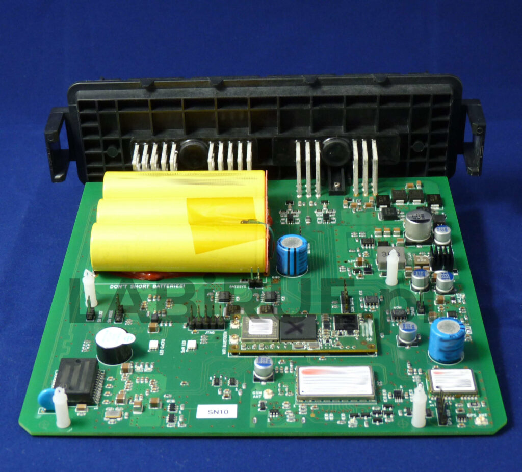
We mount SMD and THT components in semi automated way. Soldering is processed by reflow, solder bath or manually.
We can create test / programming bed with needles internally. When everything is OK board receives laser engraving and may be passed to apply conformal coating or special epoxies and owen baked and curred.
In house hw testing & reporting
We do our best when testing sample parts from different angles. Signal integrity, EMI, thermal, Converter Stability, Load responses, transfer characteristics are small section of our capabilities.
Each test we execute try to precede with good understanding and well planning to avoid respinns. Each test not ends only on pointing problems but also looks for root causes, solutions. Direct local contact between design colleagues and we can verify and document proper selection really quickly. We don’t hestitate to rework test samples.
Any questions or cooperation propositions?
We can discuss briefly your needs freely but more detailed topic investigation, solutions proposition, quotation are paid.