
As technology goes forward there is demand for higher quality of image, more data to transfer in quicker manner etc. It all results in wide usage of high speed gigabit range links.
Advantages in ADCs, DACs which are now capable to work at radio frequencies gives a lot of opportunities and flexibility in radio front-ends design causing widespread of SoftwareDefinedRadios.
All those circuits have in common oscillators and PLLs which are multiplying relatively low oscyllator frequnecy up to gigaHertz ranges. Simplified diagram of PLL is depicted below:
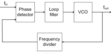
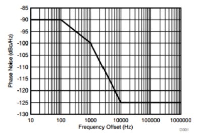
Input stage compares phase of received signal with VoltageControlledOscillator running at high frequnecies with phase from frequency divider. PLLs LowPassFilters in their feedback controll lopp have certain limitation. Those requirements are depicted in forma as phase noise vs frequency offset from main oscillator tone.
One may assume I will be clever and use fully integrated oscillator which requires only power supply and match datasheet specification with requirements of signal tollerance +/-ppm.
It is not enough.
Does all in one module oscillator has PSRR?
To perform this verification following circuit is used.
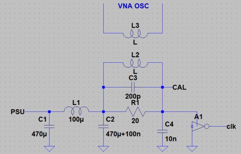
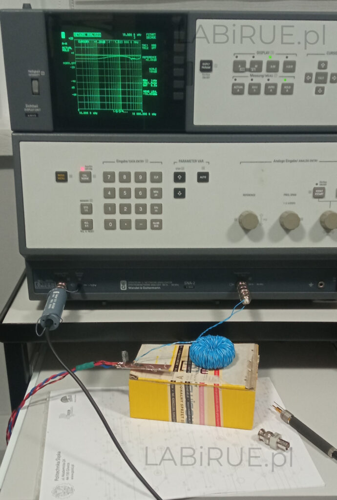
Test setup consist out of:
- Laboratory power supply AIM TTI
- Low frequency, high stability,
military grade VNA Wandell & Goltermann SNA-2 - Wideband coupling transformer 1:1.
- Active FET probe
- Test PCB board with oscillator
To measure oscillator without 50R loading instrument HiZ probe is used. Prior to measurement injection path is measured and waveform stored into VNA memory.
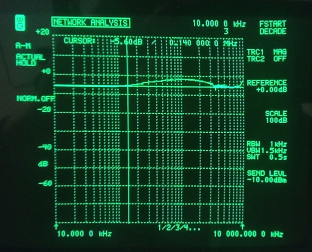
It can be stated that PSRR is almost zero at 1MHz. PSRR up to 140kHz is arround -5,6dB.
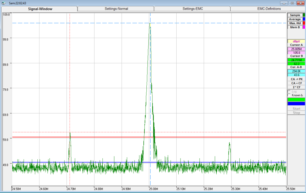
Everything what is present and introduced by most of used DCDC converters will modulate oscillator and create excessive jiiter on the PLL output.
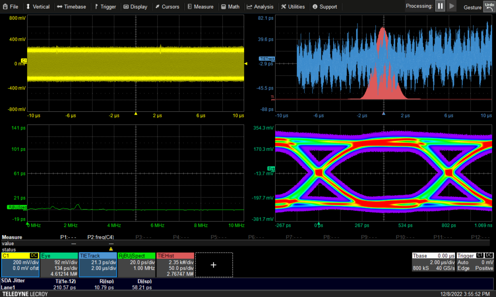
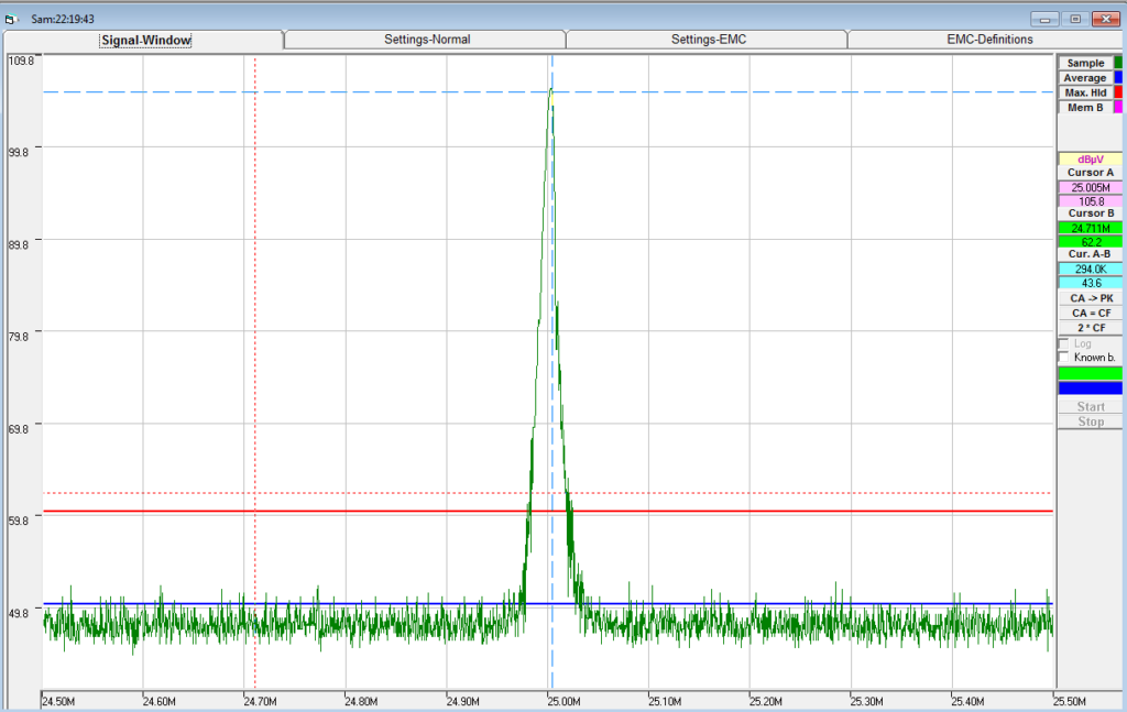
Comparison
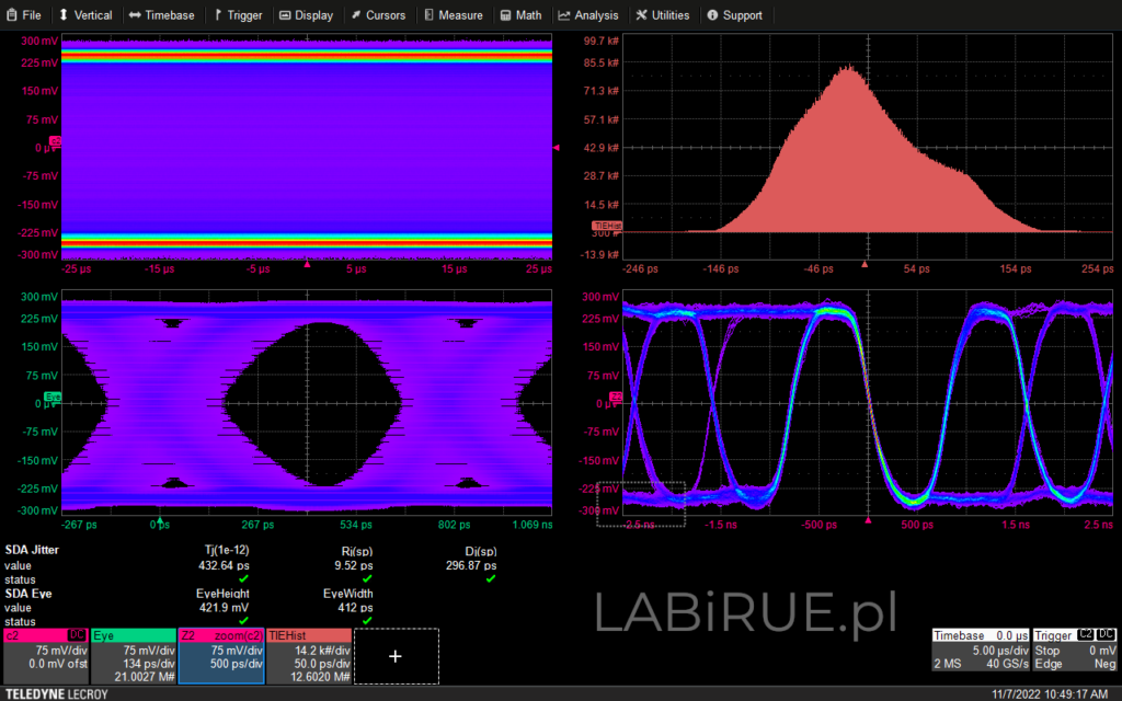
Effects of low frequency running DCDC converter injecting ripple into oscillator power rail.
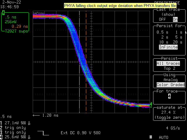
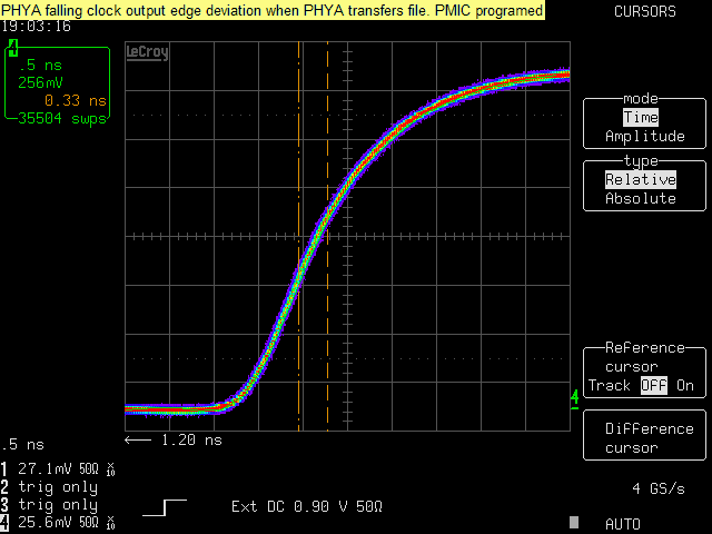
Below example shows how oscillator jiiter affects high speed SGMII link.