
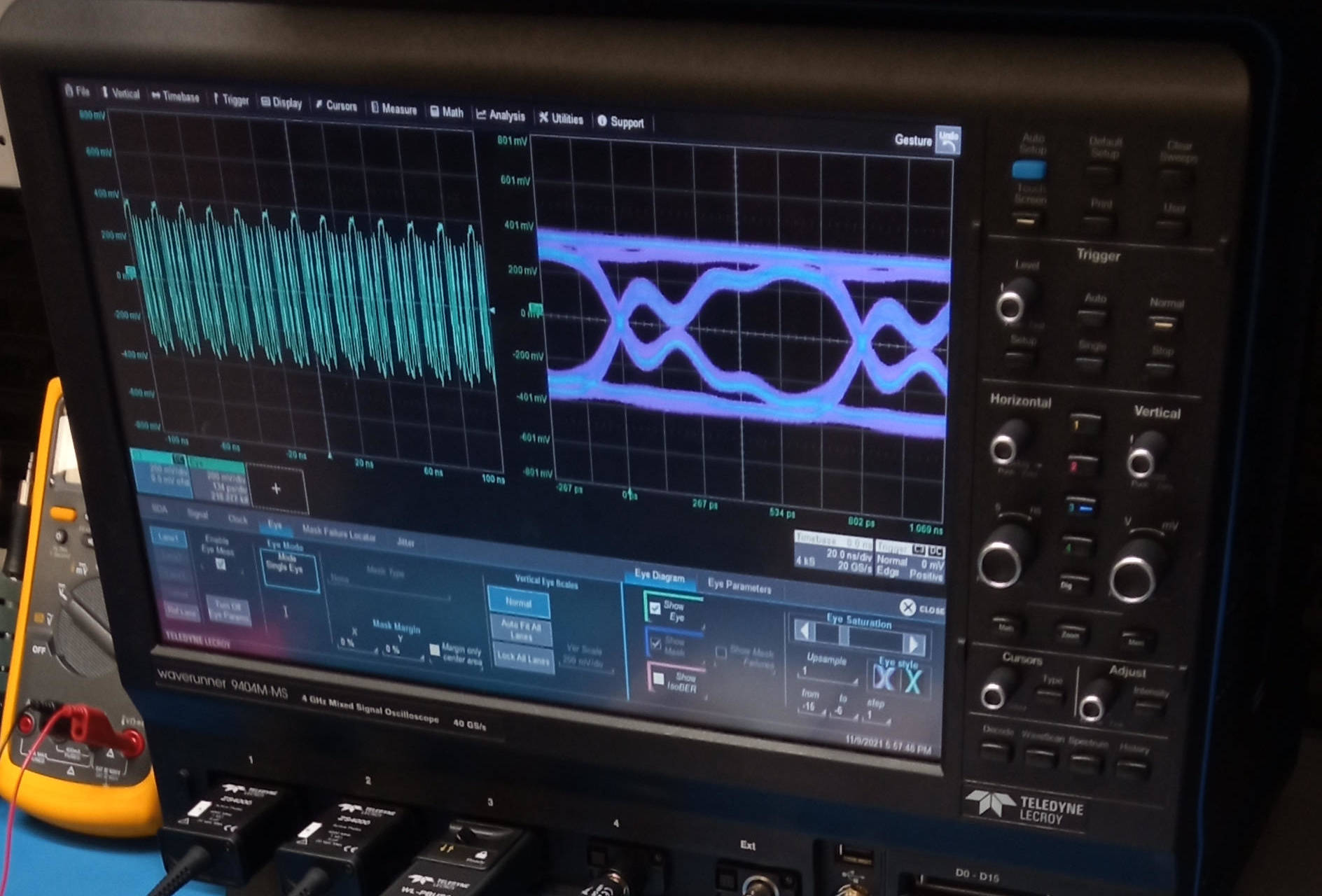
Modern embedded systems may have multigigabit speed operated connections. In professional electronics development it is not enough to see if test sample is working.
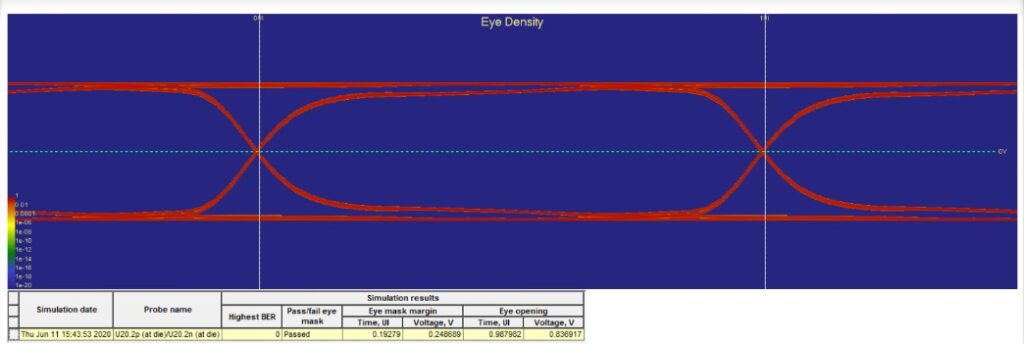
Not allways full computer singal integrity simulations are possible or they are too optimistic like depicted below:
Sometimes there is lack of connector S-parameter models and complicated elektromechanical design and we have to perform phisical measurements.
Probe placement point dilemma
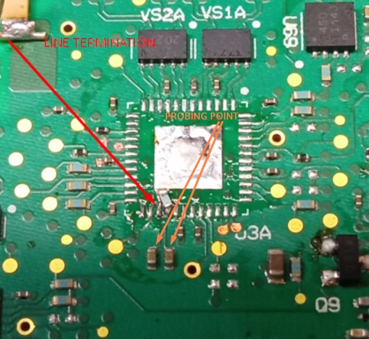
Here we are tryng to measure 1.25GHz SERDES signal. Receiver is in QFN pacakge and line AC coupling series 100nF capacitors are in about 2 length of C0402 package from IC. 100R termination in built into IC.
It is much easier to locate active HiZ differential probe there.
Our wavelength on typical PCB FR4 has 114mm when our probe location is at distance of about 2mm.
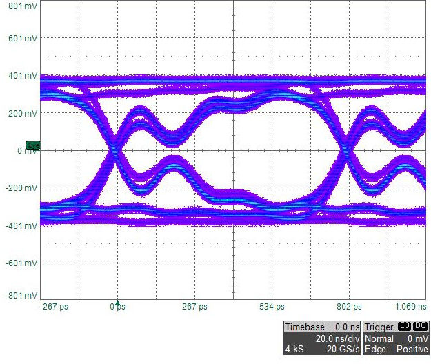
Eye diagram of SERDES captured @ AC coupling capacitors with IC present looks terribly.
Parasitic capacitance effects
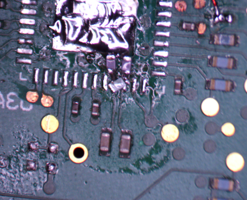
Below depicted how different parasitic capacitance to ground in receiver circuit affect measured signal shape. Capacitors connected at both ends of termination resistor located at QFN IC pins to grounded PAD under QFN IC used to simulate different conditions.
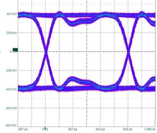
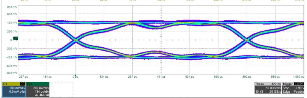
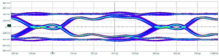
More parasitic pins capacitance, more front edge of waveform is attenuated by reflected wave.
Proper approach
There is need for forward channel simulation performed by oscilloscope called “deembedding”.
To make it happen we need to have probe tip model or the best S-parameters and also IC packaging and receiver parasitic specification.
Here we are dealing with differential pair thus 4 port S-parameters are used.
Oscilloscope gets signal from differential probe thus 2-port S-parameters are needed.
Building this signal chain in software like Keysight ADS and creating transmission channel S21 parameters we can feed them into oscilloscope to enable channel deembedding.
Finally we see that signal received internally by IC does not look so bad.
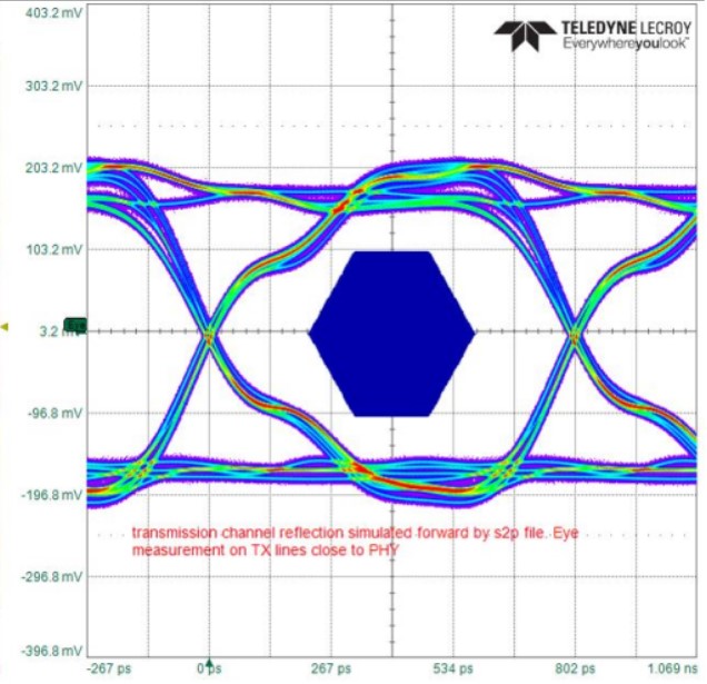
On the other hand first vendors provided simulation model does not considered internal parasites that resulted in almost perfect simulation results.